When the process of front-end production is completed then to save the chip the wafers are transmitted to the assembly facility. It brings the heat from the devices, assists the integration into the electronic systems, and confines the electric interference.
Building of wafers
In manufacturing, the semiconductor has an essential role no matter whether it is a small chip or a big motor car. In semiconductor production, the processing of chemical elements is done in the wafer form. Within the plastic cassettes, the LED Epi wafer is built up and with the specific production time, the circumstances are made out of steps.
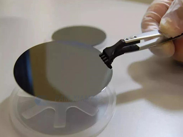
Wafer handling equipment is the emerging manufacturing process that is made to check the cleanliness and environmental control. Within the semiconductor front-end industry, it has diminished from the semiconductor devices manufacturing. For the significant environments, the process is carried out where certain factors are checked out, such as humidity, particle contamination, temperature, and controlled with the particular parameters.
To handle delicate thin wafers the bonding of the device wafer is done with a rigid carrier substrate before the back-thinning process. With the use of an adhesive bonding layer, the originally thick device wafer is bonded with its active surface to a carrier wafer.
It arrives in a consignment production form if we discuss the semiconductor backend production that is based on many customers' various orders. Picked up from the GaN LED wafers conveyed from the front-end production, the backend companies with the non-defective dies start building the final product in such a case. It makes the products reach their place within the due dates.

LED epitaxial wafer gives a detailed description of the non-repairable chips that are pushed to the next step. The defectiveness and the opposed information are filled up when this test gets completed and based on the matter it is passed through the backend process. The information conveys that only non-defective dies are taken in the final product. Wafer handling equipment is the emerging manufacturing process that is made to check the cleanliness and environmental control. Within the semiconductor front-end industry, it has diminished from the semiconductor devices manufacturing. The manufacturers, as with the bump in the semiconductor's request, turn on a further note towards automating the production process.


